Nanocluster Deposition Facility
Description
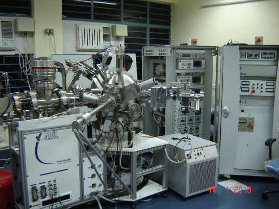
This deposition facility has been procured under a sub-project entitled “Low Energy Nanocluster Ion beam facility for novel film deposition and characterization” in the 11th Plan period of India under the project Center for Nanoscience and Surface Physics (CENSUP) of SINP. The whole set-up is a unique facility in combination of nanocluster film deposition unit (Model: Nanodep60) attached with in-situ X-ray Photoelectron Spectroscopy (XPS) facility. The nanocluster source can produce well-defined beam of nanocrystalline particles in the gas condensation method. A magnetron is used to sputter the desired material in a cooled (by liquid nitrogen) aggregation region in presence of a buffer gas. Nanoclusters of metallic, semiconductor and insulator target (with RF-mode operation) can be produced and then the mass- or size-selected clusters are obtained by using a quadrupole mass filter. The UHV end station is equipped with a number of growth and characterization facilities.
This gas aggregation type cluster source giving size-selected nanoclusters and equipped with in-situ XPS facility is the first of its kind in India.
Manufacturer
Oxford Applied Research, UK
Model
Nanocluster Source: NC200U-B
Quadrupole Mass Filter: QMF200
DC Ion Source: DC25
Installation Place and Date
Ground floor of Phase IV building
Installation date : 21st May, 2010
Major components/features of the system
1) Vacuum System: Turbo Molecular Pumps backed by Scroll pumps, Ion Pump in the XPS analyzer region
Measures of base pressures: Nanocluster source 10^(-6) mbar
Load-Lock Chamber 10^(-8) mbar
Main Chamber <5×10^(-10) mbar
2) Nanocluster Source
Material source: DC/RF Magnetron
Aggregation Length (variable): 4.8 – 14.8 cm
Aggregation tube cooling: by chilled water or L-N2
Power Supply: 1 kW DC power supply
Mean cluster size: 0.4 to 10 nm (Cu)
3) Quadrupole Mass Filter
Mass range: 50 amu to 3×10⁶ amu 3×10^6 amu
Resolution: ~2% FWHM (of the mass spec. signal)
4) Main Chamber (End-station)
(a) Load-Lock Chamber for preparation/transfer of samples
Sample movement from the load-lock chamber by magnetically coupled transfer arm
(b) DC Ion Source attached in Main Chamber
Beam energy: 100 eV to 1 keV, Beam current: ~ 40 mA at 1 keV for Ar-ions. This ion gun is used to
clean the sample surface and to etch the surface for XPS depth profiling.
(c) Goniometer for sample manipulation (Main Chamber)
2 inch diameter with heating to 800ºC, substrate rotation, Sample Bias Voltage (-5kV to +5kV DC)
and X-Y and Z movement capabilities
(d) e-Beam Evaporator (Main Chamber)
No. of pockets: 4, No co-evaporation, Maximum power dissipation 200 W
(e) Quartz-Crystal Thickness Monitor (Main Chamber)
Water-cooled quartz crystal monitor (movable) with controller.
(f) X-ray Photoelectron Spectroscopy (XPS) set up (Main Chamber)
Twin anode (Al & Mg) X-ray source (Model: VSW - TA10)
Hemispherical Analyser (Model: VSW- CL150VMMCD, 150 mm mean radius)
Please also see:
research
Description
This deposition facility has been procured under a sub-project entitled “Low Energy Nanocluster Ion beam facility for novel film deposition and characterization” in the 11th Plan period of India under the project Center for Nanoscience and Surface Physics (CENSUP) of SINP. The whole set-up is a unique facility in combination of nanocluster film deposition unit (Model: Nanodep60) attached with in-situ X-ray Photoelectron Spectroscopy (XPS) facility. The nanocluster source can produce well-defined beam of nanocrystalline particles in the gas condensation method. A magnetron is used to sputter the desired material in a cooled (by liquid nitrogen) aggregation region in presence of a buffer gas. Nanoclusters of metallic, semiconductor and insulator target (with RF-mode operation) can be produced and then the mass- or size-selected clusters are obtained by using a quadrupole mass filter. The UHV end station is equipped with a number of growth and characterization facilities.
This gas aggregation type cluster source giving size-selected nanoclusters and equipped with in-situ XPS facility is the first of its kind in India.
Manufacturer
Oxford Applied Research, UK
Model
Nanocluster Source: NC200U-B
Quadrupole Mass Filter: QMF200
DC Ion Source: DC25
Installation Place and Date
Ground floor of Phase IV building
Installation date : 21st May, 2010
Major components/features of the system
1) Vacuum System: Turbo Molecular Pumps backed by Scroll pumps, Ion Pump in the XPS analyzer region
Measures of base pressures: Nanocluster source 10^(-6) mbar
Load-Lock Chamber 10^(-8) mbar
Main Chamber <5×10^(-10) mbar
2) Nanocluster Source
Material source: DC/RF Magnetron
Aggregation Length (variable): 4.8 – 14.8 cm
Aggregation tube cooling: by chilled water or L-N2
Power Supply: 1 kW DC power supply
Mean cluster size: 0.4 to 10 nm (Cu)
3) Quadrupole Mass Filter
Mass range: 50 amu to 3×10⁶ amu 3×10^6 amu
Resolution: ~2% FWHM (of the mass spec. signal)
4) Main Chamber (End-station)
(a) Load-Lock Chamber for preparation/transfer of samples
Sample movement from the load-lock chamber by magnetically coupled transfer arm
(b) DC Ion Source attached in Main Chamber
Beam energy: 100 eV to 1 keV, Beam current: ~ 40 mA at 1 keV for Ar-ions. This ion gun is used to
clean the sample surface and to etch the surface for XPS depth profiling.
(c) Goniometer for sample manipulation (Main Chamber)
2 inch diameter with heating to 800ºC, substrate rotation, Sample Bias Voltage (-5kV to +5kV DC)
and X-Y and Z movement capabilities
(d) e-Beam Evaporator (Main Chamber)
No. of pockets: 4, No co-evaporation, Maximum power dissipation 200 W
(e) Quartz-Crystal Thickness Monitor (Main Chamber)
Water-cooled quartz crystal monitor (movable) with controller.
(f) X-ray Photoelectron Spectroscopy (XPS) set up (Main Chamber)
Twin anode (Al & Mg) X-ray source (Model: VSW - TA10)
Hemispherical Analyser (Model: VSW- CL150VMMCD, 150 mm mean radius)
Please also see:
research
